Related Posts Plugin for WordPress, Blogger...

Monday, December 30, 2013

Cable TV amplifier Circuits.

Description.
This is a very simple cable TV amplifier using two transistors. This amplifier circuit is most suitable for cable TV systems using 75 Ohm coaxial cables and works fine up to 150MHz. Transistor T1 performs the job of amplification. Up to 20dB gain can be expected from the circuit.T2 is wired as an emitter follower to increase current gain.Electronics Circuit Application


        Notes.
  • The circuit can be assembled on a Vero board.
  • Use 12V DC for powering the circuit.
  • Type no of the transistors are not very critical.
  • Any medium power NPN RF transistors can be used in place of T1 and T2.
  • This is just an elementary circuit. Do not compare it with high quality Cable TV amplifiers available in the market. Electronics Circuit Application

Sunday, December 29, 2013

Matrix LED display to 8051 microcontroller

An LED dot matrix display consists of a matrix of  LED’s arranged in a rectangular configuration. The desired character or graphics can be displayed by switching ON /OFF  a desired configuration of LED’s. Common display configurations available are 7×5, 8×8, 7×15, etc. LED dot matrix can be used in simple display applications where the resolution is not a big concern.  The figure below shows the arrangement of LEDs in a typical 7×5 dot matrix display. Electronics Circuit Application

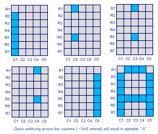
Any individual LED or a group of LEDs in the matrix can be activated by switching the required number of rows and columns. For example, in the above figure if  Row1 is made high and Column1 is made low, the top left LED (address R1C1) will glow. As a demonstration, lets see how we can display letter “A” using the display. The tables given below shows the logic levels at each pin  for displaying A. Electronics Circuit Application


 In the above diagram you can see that only one LED in a row will be ON at a time but any number of  LEDs in a column can be ON at a time.  That means the microcontroller’s port pin can directly drive a row but it requires  additional circuit for driving the column lines.  The circuit diagram for interfacing dot matrix display and 8051 microcontroller is shown below.Electronics Circuit Application


Circuit diagram
The purpose of ULN2003A here is to drive the column lines of the display. ULN2003A is a high voltage (50V), high current (500mA per channel) darlington transistor array. Each IC has 7 channels with individual output clamp diodes. ULN2003A  an active high device, which means a logic high must be applied to the input  to make the corresponding output high. The input pins are designated as 1B, 2B, 3B, 4B, 5B, 6B, 7B while corresponding output pins are designated as 1C, 2C, 3C, 4C, 5C, 6C, 7C.  The pin configuration and simplified internal logic of ULN2003A is shown in the figure below. Electronics Circuit Application
 
Program.
ORG 00H
MOV P3,#00000000B        // initializes port 3 as output port
MOV P1,#00000000B        // initializes port 1 as output port
MAIN: MOV P3,#01111110B
      MOV P1,#11111110B
      ACALL DELAY
      MOV P3,#00010001B
      MOV P1,#11111101B
      ACALL DELAY
      MOV P3,#00010001B
      MOV P1,#11111011B
      ACALL DELAY
      MOV P3,#00010001B
      MOV P1,#11110111B
      ACALL DELAY
      MOV P3,#01111110B
      MOV P1,#11101111B
      ACALL DELAY
      SJMP MAIN         // jumps back to the main loop
DELAY: MOV R6,#255D     // 1ms delay subroutine
HERE: DJNZ R6,HERE
      RET
END Electronics Circuit Application

Thursday, December 26, 2013

digitally selected output Adjustable regulator circuits

A very simple adjustable regulator circuit with digitally selected output is shown above. The circuit is a just a modification of the ordinary voltage regulator using LM317. Parallel to the resistor R4, four more resistor branches each with a transistor switch is added and these resistors can be included or excluded in to the circuit by making the corresponding switching transistor ON. In simple words the output voltage will be according to the logic level of the digital inputs A, B, C and D. Logic high at terminal A will make Q1 ON and so resistor R5 will be added parallel to R4 and so on. Addition of each resistance in parallel to the R4 will reduce the effective resistance of the path and so the output voltage of the resistance will decrease in steps. The width of each step depends on the value of the resistors you choose. Resistor R4 sets the maximum output voltage and it is according to the equation V out Max = 1.25V (1 + (R4/R3)) + (Iadj x R4).Electronics Circuit Application

Wednesday, December 25, 2013

LM317using Typical positive voltage regulator circuit

Few useful circuits using the voltage regulator IC LM317 is shown here. LM317 is a three terminal voltage regulator IC from National Semiconductors. The IC is capable of delivering up to 1A of output current. Input voltage can be up to 40V and output voltage can be adjusted from 1.2V to 37V.

 Electronics Circuit Application

Thursday, December 12, 2013

2 transistor siren circuit

The siren circuit is what importance in various alarm. For example : the emergency alert, burglar alarm circuits, Fire alarm circuits, Timer , sensor controls, etc. If we have not these circuit, We will not able to recognize the functionality of the circuit,we set out.
Operation of the circuit is Q1 and Q2 will work with R3, R4 and C2 is a frequency generator circuit with output connected to LED1 and speakers SP1. When I press the switch S1 to the C1 will begin to charge allows the voltage to pin B of Q1 increase other. The Q1 is working and Q2 is working with at the C1 charge full cycle will stop oscillator speaker is not.
The LED1 light and hold the release the pressure switch S1, resulting in C1 will start discharger through R3, Q1 to ground. The oscillator circuit sound Sirens in the lower out. If we press the switch S1 and then quickly leave many. The sound will be as continuous as C1 to charge and discharge alternately continuously.Electronics Circuit Application
circuits diagram
 

Wednesday, December 11, 2013

5V 1A Switching regulator by IC LM2575-5 Circuits

The switching regulator which used LM2575-5.0 in this page. You can make the stable voltage by using the 3 terminal regulator like LM317. However, because the output electric current and the inputted electric current are the same approximately, the difference between the input electric power (The input voltage x The input electric current) and the output power (The output voltage x The output current) is consumed as the heat with the regulator. Because it is, the efficiency isn’t good.


Data sheet for LM2575

Monday, December 9, 2013

LM3909 using 1.5V Battery or 3V Monitor circuits

We come to add LED Flasher for Monitor the electric current of battery 1.5V and 3V. By use the integrated circuit LED Flasher or Oscillator. By the rate something flasher equal to 2V. This circuit eats electric a little current poor age the work of battery long can’t be like be usable. If friends use battery 3V as a result liberate pin 1 float keep. I hope that a friend may apply with Battery 1.5V or 3V Monitor Circuit

LM334 using Voltage Reference Circuits.

This Voltage Reference Circuit. It used LM334 (ADJUSTABLE CURRENT SOURCES IC)
By fix the trend is stable. It make the pressure that pay to come out have tall stability. By can fine decorate VR1 10K Adjust Voltage Output. And You can use Voltage Input power supply at +2.5V to +20V. cause be high class voltage Output be valuable 0.8-5.0V depend on fining decorates VR1 there.
LM334  cicuits

Wednesday, December 4, 2013

How to huawei hsdpa usb modem service ?

Powered by
Electronics Circuit Application
www.electronicsyard.blogspot.com

2N4851 Using 12V Battery charger Circuit

This is an automatic 12V battery charger circuit, they uses the power SCR and UJT are main parts.
And they will not work except the battery 12V to be charged with right polarity, so prevent errors as well. The battery voltage controls the charger and when the battery is fully charged, the charger will not supply current to the battery anymore.
2N4851


 The battery charging current through the SCR MCR3818, when it is triggered into the conducting state by the UJT 2N4851 relaxation oscillator. And the oscillator is only activated when the battery voltage is low. Vb2b1 of the UJT derive the battery voltage that to be charged, and since Vp = Vd = Vb2b1 ; the higher Vb2b1, the higher Vp. When Vp exceeds the breakdown voltage of the zener diode ZD1, the UJT will stop to work and the SCR1 will not conduct.
T1 =Primary – 30 turn #22 , Secondary – 45 turns #22
R1 = Series resistance to limit current through SCR so use MCR3818 at 20 amps.
The setting VR1, we can charge the battery as needed. Electronics Circuit Application

Tuesday, December 3, 2013

M7555 - Battery Status Monitor circuit

The low power LED flasher by ICM7555
Normally, when you need to use LED display status of the battery 6V-12V. Just add a resistor in series only. It is easy and saving.
But not cool and consumes more power.
- The impression of a bright that continuously. I think that did not noticeable it.
- When the LED light as well So consumes too much energy. Although the LED need voltage is 1.8V only, but it uses too current is 15mA-20mA.
A wise choice.
- The LED flashes very prominent.
- Find out how to use current less than 1mA. When several ten years ago. I’ve used a LM3909 of LED Flasher/Oscillator IC.It is built for a particular flashing light or low current led flasher so easy to make and includes a very small amount. But unfortunately. Now IC manufacturers stopped producing it.
But we also have the option of interest, may be better than. If you are familiar with the IC 555 is a relative of the family is ICM7555 (or 7555IPA) with the same features. However very low power consumption. Because the internal structure of CMOS, So works great.
You take a look that the circuit is easy like I said or not. As shown below. You see not wrong, it using only three pieces, it can make the LED to flashes. By pull current from the power supply is only 0.15mA. It is designed as a typical Stable multivibrators circuit. (If you do not understand see this web. We have several circuits)
Special! In normal circuit, the capacitor will discharge directly to ground. However, for this circuit, the capacitor is discharged through LED1, so that LED1 flashes intermittently.
Just this you have a simple battery monitor circuit by IPM7555 Some people would say that’s not worth it. This circuit is more expensive than the old method. However it can extend battery life by several times, or Adapted for low current power supply such as solar or other alternative energy sources. They result is the same. Electronics Circuit Application

Monday, December 2, 2013

Car brake lights by BC327 Circuits

his is the circuit add beauty to the brake lights of the car. With a display of 14 LEDs, visible clearly, for safety and beautiful. The installation format can fix by oneself as you like it.
This circuit use the astable multivibrator for generate a oscillate frequency so all LED flashing.

The working of the circuits
When enter the light brake voltage, makes have power supply 12V come in cause LED6-LED9 glow or On. Besides the trend will flow to change R2 go to bias pin base of Q1-BC327 PNP transistor and Q2-BC327, causes LED1-LED5 and LED11-LED14 the bright up. Which there are R1 and R3 help to limit a current that flow through LEDs enough liberate brake power supply 12V disappear make LED every switch off.


 parst list
Q1,Q2_______________BC327____50V 1A PNP transistorrs
LED1-LED14__________LED display as you want.
R1,R4_______________22 ohms 0.5 watts 5% resistors
R2__________________390 ohms_0.5 watts 5% resistors
R3__________________500 ohms__0.5 watts 5% resistors Electronics Circuit Application

Amplifier speakers delay circuits

This circuit is small-sized circuit at can build easy, and usable get easy between a loudspeaker with amplifier. By have relay be switch edit during opening-time switch that stereo will hear the sound “Tlub” come out from loudspeaker. Which this sound is sound the electricity will pull sharply to flow enter still a loudspeaker and may will make a loudspeaker can are damaged therefore then necessary to must have time drag while open switch for a moment. For speak this part disappear before then build enter still a loudspeaker.

When receive power supply come in, The C1 will charge thereafter C2 begin charge change R1. When C2 charge full until go to bias give Q1 work go to current driver give relay. Which use relay model double contract, make contract switch touch. From that time build a loudspeaker suits power amplifier the period will delay to depend on the value C2. If want to give can delay long ago enhance the value C2. But if give can delay short down devalue C2.
Now, You do want to make this project. Electronics Circuit Application

Saturday, November 30, 2013

Audio Amplifier 11 watt using TDA1554

This is a simple circuit. Just use a single IC, but the amplifier has 4 channels, 11 channels per watt, which is Philip IC TDA1554 number suitable for listening at home or in any vehicle. Just because the power supply 12-15 volt or will be used to expand any home theater sound system. The first 2-channel amplifier front speakers. And 2 to extend the back surround sound speakers also.

This circuit power supply 12 volts to 18 volts Power consumption at 5A. The input 4 input pins 1, 2, 17 and 18 is divided into a horizontal input inverter Ting 2 channels (Pin 1, 17). inverse model and input object 2 channels (pins 2, 6). That we can use that. To output phase to phase or did not return. The output will be the fourth slot on the leg 6, 8, 12, 10, with a C7-C10 serves to increase the low frequency stability better before you go to the speaker. The switch S1 acts on mute by pressing S1 will be closed sound system circuit in Mute, and if open circuit S1 standby ready to work. The C5 and C6 will filter light to smooth out and eliminate interference. Electronics Circuit Application

Thursday, November 28, 2013

Switch-Mode DC-DC Converter Circuits.

This circuit is based on mobile phone chargers. These chargers are based on the Motorola MC34063 switchmode IC. By changing the values of the feedback resistors (R1 & R2), the output voltage can be varied over a wide range. Just modify R1 and R2 according to the formula: Vout = 1.25 (1+R2/R1). The values shown give an output of 3V.Electronics Circuit Application

Switch-mode DC-DC Converter Circuit Diagram

 Electronics Circuit Application

Wednesday, November 27, 2013

Bird Bath Fountain Monitor circuits

A bird bath fountain (a small shallow pond-created with a water-filled basin- in which birds may bath and from which they may drink) can be a garden ornament, small reflecting pool, outdoor sculpture, and part of creating a vital wildlife garden. It is an attraction for many different species of birds to visit gardens, especially during the summer and drought periods. This fountains that provide a reliable source of water year round add to the popularity and micro-habitat support. Presented here ia an “add-on” electronics circuit for bird water baths.

The circuit constantly monitor the water level in the bath, and brings up an audio&visual warning signal when its sensor probe notices that the water level is very low, or the bath is in dry state. It can be powered from any 9VDC adaptor or similar power source.
After construction, fit out the sensor probe inside the bird bath in an appropriate position and connect it to the remotely-located (usually inside the house) master circuit using high-quality twisted-pair/flat cable. The sensor probe can be constructed from a pair of new injection needles. The needles should be firmly fixed about 10 mm apart on a piece of laminated plastic sheet.

Working of this circuit is very simple! Here, a “gimmick” potential divider ( P1, R5 and the sensor probe J1) is wired at the base of transistor T1 (BC547) to switch it on when water is available between the needles of the sensor probe (J1). Conduction of T1 pulls down the reset terminal (pin 4) of the astable oscillator IC1 (LM555) and hence the astable is disabled in standby state. Potentiometer P1 (1M) sets the threshold level.
But when the sensor probe is dry, IC1 is enabled by R1 (4K7) and the piezo-buzzer (BZ1) starts beeping at near 3Hz rate. Red LED serves as a flaunting visual indicator. Electronics Circuit Application

Monday, November 25, 2013

MC34063 Switch-Mode DC-DC Converter

This circuit is based on mobile phone chargers. These chargers are based on the Motorola MC34063 switchmode IC. By changing the values of the feedback resistors (R1 & R2), the output voltage can be varied over a wide range. Just modify R1 and R2 according to the formula: Vout = 1.25 (1+R2/R1). The values shown give an output of 3V.

DC-DC Converter Circuit Diagram


Input voltage

Output voltage

Sunday, November 24, 2013

ZTE WP826A CDMA fixed wireless phone


ZTE WP826A CDMA fixed wireless phone Data Cable Connector Replacement
Electronics Circuit Application

Phone Broadcaster Circuits

Here is a simple yet very useful circuit which can be used to eavesdrop on a telephone conversation. The circuit can also be used as a wireless telephone amplifier. 


One important feature of this circuit is that the circuit derives its power directly from the active telephone lines, and thus avoids use of any external battery or other power supplies. This not only saves a lot of space but also money. It consumes very low current from telephone lines without disturbing its performance. The circuit is very tiny and can be built using a single-IC type veroboard that can be easily fitted inside a telephone connection box of 3.75 cm x 5 cm.


Saturday, November 23, 2013

TDA2030 using Amplifier Circuits

This The multi-purpose Amplifier using TDA2030. It is have power 8 watt (RMS) at 8 ohm loudspeakers. It is have low noise be valuable THD (Total harmonic distortion) 0.1% , When friends use Power supply Voltage Source 28 Volt at 4 ohm loudspeakers have output power 12Watt. But be high class the noise increases to are 2 times. Besides still three be usable with Volt supply about 9Volt , but there is the electric power is down respectively. The VR1 use for Volume popularity level of sound signal. By if a friend can’t seek 22K values use 50K values can replace. For other detail about the integrated circuit TDA2030 IC and other , friends see in the circuit better yes.
TDA2030 using Amplifier
 Electronics Circuit Application

Friday, November 22, 2013

Speaker protection circuit

Why to have The speaker protection circuit? How do the speaker protection circuit can prevent
For the power amplifier circuit in the new version, usually popular to build by the direct coupling circuit, from the the amplifier circuit to the speakers directly, or as also known as the OCL amplifier circuit. Which this pattern are both positive and negative power supply circuit, or what I call is the three wire power.
Features of this circuit has the advantage is that the frequency response is better than any other circuit. But it has the disadvantage that when the circuit is damages. In any case, it may be has a DC voltage positive or negative that the higher like the power supply, output to Immediately the speakers.
With this voltage, will make coil of the speaker is burned and lack of eventually, so if we do not want to the speaker is usually the most expensive audio system, need to damaged. We need to do is cut this voltage not go out the speaker. We call this circuit. Speaker protection circuit. As shown below.
the speakers? This may be questions understand of somebody, and if you have not yet received a satisfactory answer, here is the answer.

Working of circuit
As shown in this circuit, we take a some signal from the speaker enter through the resistors R1, R2 into the protection speakers section, By reducing the signal strength lower down, then after the capacitor C1 serves to bypass this signal to ground.
However, if the dc voltage to either positive or negative, whatever this voltage is passed through the bridge diode circuit immediately, by they will be setting voltage input is positive or negative to the positive voltage to the base pin of Q1 doing the Q1 work.
When the Q1 working, will make the collector voltage low down, the bias voltage at base pin of Q2 will also lower down, making The Q2,Q3 stop run therefore not have current pass through the relay RY1, so it will be cut off the signal of power amplifier without to output speaker at once. The speakers will safe from the dc power.
To be used.
1. to connect the ground wire from the amplifier to ground of the protection speaker.
2. to connect the signal output from the the amplifier to the speakers,we connected it to the IN of the protection speaker to both the left and right.
3. to connect the OUT signal from the speaker to the positive terminal of the protection speaker.
To build and test circuit.
1.To produce the correct devices in the PCB. as Figure 2
2.Check the soldering is done at every point.
3.Test the functionality of circuit. By connected power supply circuit. And see the LED to stick and hear a click with the relay working.
4.Experiments, connected DC voltage at the IN of the anti-speakers, the LED will extinguish along with the relay will stop immediately. If you do not follow this. Show that a failure occurs. Make sure to found before it is available.

 Electronics Circuit Application

Thursday, November 21, 2013

Huawei E1750 HSDPA usb modem service.

Powered by
Electronics Circuit Application
www.electronicsyard.blogspot.com

FM receiver circuits and using LM386 amplifier

This is one of the simplest ways of making an FM receiver. Just get a low cost FM receiver kit, make an audio amplifier using LM386, connect them together and your FM receiver is ready.

Most of the commercial FM receiver kits receive the signals within the FM band, usually 88-108 MHz.

This project is for novices who can make projects on breadboard.

If you have never made an Audio amplifier, please try this: LM386 on breadboard. The tutorial shows you all the connections.

The FM receiver kit usually comes with 4 wires: +6V, GND, Antenna and Audio. You need to connect the ‘Audio‘ wire to the ‘input’ pin of the audio amplifier circuit.


Schematic of Audio Amplifier using LM386:

battery charger Circuits


 Description.
A simple battery charger based on SCR is shown here.Here the SCR rectifies the AC mains voltage to charge the battery.When the battery connected to the charger gets discharged the battery voltage gets dropped.This inhibits the forward biasing voltage from reaching the base of the transistor Q1 through R4 and D2.This switches off the transistor.When the transistor is turned OFF,the gate of SCR (H1) gets the triggering voltage via R1 & D3.This makes the SCR to conduct and it starts to rectify the AC input voltage.The rectified voltage is given to the battery through the resistor R6(5W).This starts charging of the  battery.
When the battery is completely charged the base of Q1 gets the forward bias signal through the voltage divider circuit made of R3,R4,R5 and D2.This turns the transistor ON.When the Q1 is turned ON the trigger voltage at the gate of SCR is cut off and the SCR is turned OFF.In this condition a very small amount of charge reaches the battery via R2 and D4 for trickle charging.Since the charging voltage is only half wave rectified ,this type of charger is suitable only for slow charging.For fast charging full wave rectified charging voltage is needed.

battery charger


Notes. 
  • Assemble the circuit on a good quality PCB or common board.
  • The transformer T1 can be 230V primary, 18V /3A secondary step down transformer.
  • The voltage of the battery at which the charging should stop can be set by  the POT R4.
  • The battery can be connected to the charger circuit by using crocodile clips.

Monday, November 18, 2013

kodak easyshare ls743 e45 error solution lesson 05

 
kodak easyshare ls743 e45 error solution lesson.05
next level lessons
Electronics Circuit Application

Transformerless Power Supply Circuits.

Important Notice
Electric Shock Hazard. In the UK,the neutral wire is connected to earth at the power station. If you touch the "Live" wire, then depending on how well earthed you are, you form a conductive path between Live and Neutral. DO NOT TOUCH the output of this power supply. Whilst the output of this circuit sits innocently at 12V with respect to (wrt) the other terminal, it is also 12V above earth potential. Should a component fail then either terminal will become a potential shock hazard.

Below is a project by Ron J, please heed the caution above and Ron's design notes

 If you are not experienced in dealing with it, then leave this project alone.Although Mains equipment can itself consume a lot of current, the circuits we build to control it, usually only require a few milliamps. Yet the low voltage power supply is frequently the largest part of the construction and a sizeable portion of the cost. 

Sunday, November 17, 2013

ZTE CDMA Phone data Port Repair.


MY video 
ZTE WP826A CDMA fixed wireless phoneData Cable Connector Replacement
Electronics Circuit Application


Automatic 12V Lead Acid Battery Charger circuits. 01

This charger will charge any 12V lead acid battery including flooded, gel and AGM. It is fully automatic and will charge at a rate up to about 4A until the battery voltage reaches a preset point at which it will switch to a very low current float charge. If the battery voltage drops again the charger will begin charging until the voltage once again reaches the cut off point. In this way it can be left connected to a battery indefinitely to maintain full charge without causing damage. An LED indicates when the battery is fully charged

                           circuits diagram


                                parts


Notes

  1. R2 will have to be adjusted to set the proper finish charge voltage. Flooded and gel batteries are generally charged to 13.8V. If you are cycling the battery (AGM or gel) then 14.5V to 14.9V is generally recommended by battery manufacturers. To set up the charger, set the pot to midway, turn on the charger and then connect a battery to it's output. Monitor the charge with a voltmeter until the battery reaches the proper end voltage and then adjust the pot until the LED glows steadily. The charger has now been set. To charge multiple battery types you can mount the pot on the front of the case and have each position marked for the appropriate voltage.
  2. Q1 will need a heatsink. If the circuit is mounted in a case then a small fan might be necessary and can generally be powered right off the output of D1.
  3. T1 is a transformer with a primary voltage appropriate to your location (120V, 220V, etc.) and a secondary around 12V. Using a higher voltage secondary (16V-18V) will allow you to charge 16V batteries sometimes used in racing applications.
  4. If the circuit is powered off, the battery should be disconnected from it's output otherwise the circuit will drain the battery slowly. Electronics Circuit Application

Saturday, November 16, 2013

kodak easyshare ls743 e45 Error

 
Electronics Circuit Application
         Powered by
www.electronicsyard.blogspot.com

china Bird V20 mobile phone Repair


Electronics Circuit Application
         Powered by

Mini Alarm Circuits.

This circuit, enclosed in a small plastic box, can be placed into a bag or handbag. A small magnet is placed close to the reed switch and connected to the hand or the clothes of the person carrying the bag by means of a tiny cord. If the bag is snatched abruptly, the magnet looses its contact with the reed switch, SW1 opens, the circuit starts oscillating and the loudspeaker emits a loud alarm sound. A complementary transistor-pair is wired as a high efficiency oscillator, directly driving a small loudspeaker. Low part-count and 3V battery supply allow a very compact construction. Electronics Circuit Application


Parts:

R1 = 330K
R2 = 100R
C1 = 10nF-63V
C2 = 100uF-25V
Q1 = BC547
Q2 = BC327
B1 = 3V Battery or Two AA Cells in Series
SW1 = Read Switch & Small Magnet
SPKR = 8R Loudspeaker (See Notes)


Notes:
  • The loudspeaker can be any type; its dimensions are limited only by the box that will enclose it.
  • An on-off switch is unnecessary because the stand-by current drawing is less than 20µA.
  • Current consumption when the alarm is sounding is about 100mA.
  • If the circuit is used as anti-bag-snatching, SW1 can be replaced by a 3.5mm mono Jack socket and the magnet by a 3.5mm. Mono Jack plugs having its internal leads shorted. The Jack plug will be connected to the tiny cord etc.
  • Do not supply this circuit at voltages exceeding 4.5V: it will not work and Q2 could be damaged. In any case a 3V supply is the best compromise.Electronics Circuit Application

Thursday, November 14, 2013

How to ZTE CDMA Phone data Port Repair.

ZTE WP826A CDMA fixed wireless phoneData Cable Connector Replacement
Electronics Circuit Application My you tube video

Monday, November 11, 2013

How to Replace IC (Chips)

How to Replace IC Chips.How to Replace IC Chips. Electronic repair often requires the removal and replacement of integrated circuits for Electronics Circuit Application
www.electronicsyard.blogspot.com

huawei hsdpa usb modem service

 
Powered by
Electronics Circuit Application
www.electronicsyard.blogspot.com

Friday, November 8, 2013

High Gain Wi-fi Antenna project

Presented here may be a versatile, durable, and rather distinctive Wisconsin fi antenna which will greatly extend your wireless networking vary and speed. once designed with 10 or a lot of turns, this coiling Wisconsin fi antenna immensely outperforms the cantennas and Wisconsin fi pan tiptop typically seen on the web. a brief 5 flip coiling makes a awfully smart feeder for a Wisconsin fi parabolic directional antenna. A special quality of this antenna is that it radiates and receives a circularly polarized signal. It doesn't favor vertically or horizontally polarized signals. Thus, this antenna works well Wisconsinth wi fi signals reflective off of buildings, moving vehicles, or antennas orientated at odd angles. Circularly polarized signals ar less suffering from rain, thus you'll be able to reach distant access points in stormy weather. there's a three decibel loss of gain once exploitation this antenna with linearly polarized signals; high gain is maintained by creating the antenna long - a minimum of 10 turns for complete usage.

At this point you should have a PC board with a circle in the center, four tick marks on the circle at 90 deg intervals, and one tick mark exactly between two others

PARTS REQUIRED FOR THE WIFI HELICAL ANTENNA:

  1. one square piece of copper sheet metal or single sided PC board for a ground plane.
  2. one PVC kitchen drain tailpiece (3.8 cm / 1.5" diameter) to hold the helical windings
  3. six 1/8" plastic cable ties
  4. a length of copper circuit tape (adhesive backed, width 3mm or 1/8") or #14 copper wire
  5. one suitable chassis connector (I used a reverse sma type matching the connector on my adaptor)
  6. one 90 degree angle bracket with screws and bolts to fit

CONSTRUCTION:

  1. Center the tailpiece on the PC board, copper side, and mark the circumference in ink.
  2. Mark four locations on the circumference, spaced 90 degrees, where the cable ties will hold down the PVC tube.
  3. Mark one location on the circumference, exactly between two 90 degree markings, where the coaxial connector will be mounted. 

At this point you should have a PC board with a circle in the center, four tick marks on the circle at 90 deg intervals, and one tick mark exactly between two others.


  1. Drill 1/8" holes on the inside and outside of the circumference at the cable tie locations.
  2. Drill a hole directly on the circumference suitable for the chassis connector. Carefully measure and drill other holes for this connector if necessary.
  3. Drill four holes, spaced 90 deg apart near the bottom end of the PVC tailpiece.
  4. Drill holes to accomodate a small 90 degree corner bracket.
  5. Drill holes on opposite side of board to accomodate USB wi-fi adapter that will be affixed with cable ties.
  6. Tin the copper around the connector mounting hole, then mount the connector. Clip the center pin to keep it only long enough for connection to the helix windings.
  7. Cut out a notch to accomodate the connector; it should clear center conductor, but avoud cutting out excess PVC material.
  8. Feed cable ties through from the back side of the board, through holes in the tube, and back through the board. Tighten the cable ties, making sure the tube is firmly held to the copper ground plane.
  9. Use a ruler and the edge of a sheet of paper to create a template for positioning the windings on the PVC tube. Distance zero represents the ground plane, then add the feedpoint distance, then ticks matching the turns spacing. Use the template to mark your tube on both the feedpoint side and the opposite side.
Space the turns 2.5 cm on a
tube of 3.9cm outer diameter.
Here is a table used for my prototype helical wi-fi antenna and its connector. Note that turn 1 starts at 0.8 cm (height above ground plane of feedpoint). Turns Spacing is 2.5 cm, and the diameter is 3.9 cm (close enough for 1.5" PVC tailpiece). If your connector can be trimmed to allow a feed connection closer to the ground plane than 0.8CM, then simply run the helix as low as necessary. Most impartant is keeping the proper spacing between turns.

Spacing=2.5cm
Diameter=3.9cm
(fits 1.5" PVC tailpiece)
Turn # Height (cm) above
groundplane
Half Turns
Height (cm)
1 (feedpoint) 0.8 2.05
2 3.3 4.55
3 5.8 7.05
4 8.3 9.55
5 10.8 12.05
6 13.3 14.55
7 15.8 17.05
8 18.3 19.55
9 20.8 22.05
10 23.3 24.55
11 25.8 27.05
12 28.3 29.55
13 30.8 32.05


  1. Carefully wind the helix, using circuit tape or wire, then solder to center conductor of chassis connector. Double check against the turns template. Polarization will be right-handed if the turns spiral clockwise (looking outward from feedpoint). 
  14. Attach the angle bracket and wi-fi adapter, making sure all parts are secure and ready for service, as seen in the images below. 
 The high gain wi-fi helical antenna.
10 turn stand alone version
Cable losses avoided by
mounting wi-fi adapter
at base of antenna. 
Short wi-fi helix feeding a long range parabolic wi-fi
antenna.
At this point, helical wi-fi antenna is ready for its smoke test...plug in the cables and look for some signals! Theoretical gain of the prototype helical was about 18 dB over an isotropic radiator; it beat my biquad by about 7 to 13 RSSI units, and indeed seemed less sensitive to polarization and rainfall. Signals still seem to fluctuate much from second to second. If your antenna is functioning satisfactorily at this point, I suggest spray painting three layers of clearcoat onto the windings and groundplane for stability and corrosion prevention.
 Electronics Circuit Application

Thursday, November 7, 2013

HTC mytouch 3g phones display Replace


My Projects Video>>

 Electronics Circuit Application

Power Buzzer Circuits

How typically on the average does one got to decision members of your family day after day to inform them that dinner is prepared, it’s time to go away, and also the like? The person you would like is sometimes in a very completely different space, like the hobby space or chamber. a robust buzzer within the space, combined with a pushbutton at rock bottom of the steps or within the room, may be terribly handy in such things. the center of this circuit is made by IC1, a TDA2030. This IC has inherent thermal protection, therefore it’s not going to quickly quit the ghost. R1 and R2 apply a voltage up to 0.5 the provision voltage to the and input of the opamp. R3 provides regeneration. Finally, the mix of C2, R4 and trimmer P12 determines the oscillation frequency of the circuit.
The frequency of the tone also can be adjusted victimisation P1. there's no volume management, since you usually wish to induce attention after you press pushbutton S1. match the complete circuit wherever you would like to possess the pushbutton. The loudspeaker system will then be placed in a very strategic location, like within the chamber or where is suitable. Use speaker cable to attach the loudspeaker system. traditional bell wire will cause a significant power loss if the loudspeaker system is comparatively far-off. The loudspeaker system should be ready to handle a continual power of a minimum of vi W (with a 20-V offer voltage).

Wednesday, November 6, 2013

Preamplifier Tone Control Circuits


Parts:

P1,P2___________10K  Linear Potentiometers
                     (twin concentric-spindle dual gang for stereo)

R1_____________100K  1/4W Resistor
R2,R6___________18K  1/4W Resistors
R3_______________3K3 1/4W Resistor (18K for shelving curves: see Notes)
R4,R5____________1K8 1/4W Resistors (10K for shelving curves: see Notes)
R7_____________560R  1/4W Resistor

C1_______________1µF  63V Polyester Capacitor
C2_______________4n7  63V Polyester Capacitor (3n3 for shelving curves: see Notes)
C3_______________1µ5  63V Polyester Capacitor (100nF for shelving curves: see Notes)
C4,C7__________100nF  63V Polyester Capacitors
C5,C8___________22µF  25V Electrolytic Capacitors
C6,C9_________2200µF  25V Electrolytic Capacitors

IC1___________TL072   Dual BIFET Op-Amp
IC2___________78L15   15V 100mA Positive Regulator IC
IC3___________79L15   15V 100mA Negative Regulator IC

D1,D2________1N4002  200V 1A Diodes

SW1____________DPST  Toggle Switch

J1,J2__________RCA audio input sockets
J3_____________Mini DC Power Socket


Comments:

Needing a Tone Control, this module can be inserted in the chain between the Control Center and the Power Amplifier.
The circuit is based on an original design of Reg Williamson, published on Electronics World + Wireless World, Circuit Ideas, January 1991.
This tone control circuit will take the form of either the traditional bass and treble adjustment or the shelving type, which is similar to a "tilt" control but with independent bass and treble.
Asymptotic slopes for both are about 4dB/octave, but begin to flatten out at 100Hz and 10kHz, reaching a maximum of ±15dB at the ends of the audio band.
Component values in parenthesis are those for the shelving type of control. In this case, the shelf begins at about 250Hz and 4kHz, flattening to a ±6dB maximum an octave above or below; the central point is 1kHz.
Reactive elements for the low end include a generalized impedance converter, which simulates an inductor in series with a resistor (gyrator).
When set to the electrical centers of their respective controls, the reactive elements of the equalizers are virtually out of circuit. With these settings, the circuit behaves as a unity gain amplifier with 100% negative feedback. Even so, reactive elements can be switched out altogether with a DPST on/off switch.
As with the other modules of this series, each electronic board can be fitted into a standard enclosure: Hammond extruded aluminum cases are well suited to host the boards of this preamp. In particular, the cases sized 16 x 10.3 x 5.3 cm or 22 x 10.3 x 5.3 cm have a very good look when stacked. See below an example of the possible arrangement of the front and rear panels of this module.

Notes:

  • To build the shelving type of control, use the values shown in parenthesis for R3, R4, R5, C2 and C3
  • The circuit diagram shows the Left channel only and the power supply.
  • Some parts are in common to both channels and must not be doubled. These parts are: P1 and P2 (if twin concentric-spindle dual gang potentiometers are used), IC2, IC3, C4, C5, C6, C7, C8, C9, D1, D2 and J3.
  • This module requires an external 15 - 18V ac (50mA minimum) Power Supply Adaptor.

Monday, November 4, 2013

Battery Powered 12V LED Spotlight - 12V Power Supply circuits

Most of the electronic projects and electronic devices are required 12V power source; typically a 12V sealed lead acid battery or AC powered power supply. These are typically large, heavy, difficult to handle, and expensive; portability is less. The best solution is to use a DC-DC Step up converter. These types of convertors are inexpensive, light weight and easy to use. Also provides power management and easy to work with renewable energy sources.


The input power source could be rechargeable AA batteries. Let’s make an environment friendly 12V/130mA power supply
 Electronics Circuit Application  


 100uf Electrolytic Capacitor 16V C1,C2 -2
100Ohms Resistor 1/4W R1,R2 -2
1N5817 Schotkey Diode 1A D1- 1
150UH Radial Power Inductor 1A IND1- 1
LT1073CN8-12 IC DIP Package IC1 -1
IC Base 8 PIN -1
PCB to Wire Connector- 2
4AA Battery Holder- 1

The heart of this application is LT1073 IC. It is a power management IC which steps up low voltage into high voltage by switching.

First I etched four PCBs for the prototype using a PCB design software and some other tools. The PCBs are very small (4cmX2cm) because components need to be solder as close as to the IC; because of the performance issues. I made ground copper track as wide as possible.

Now my prototype works fine and I decided to make the PCB in large quantity. I did some changes and sent my PCB file to a local PCB production company and first I got 100 pieces of PCBs. The PCBs are in good quality with solder spots and copper shield; easy to solder

 Ratings:
Operating Hours: 20,000 hours
Operating Voltage: 12V
Intensity: 55,000 mcd
Forward Current: 80 mA @ 12Vdc
Viewing Angle: 30 Degrees

Absolute Maximum Ratings:
Operating Voltage(V): 14 V
Operating Temperature (Topr): -25oC to +85oC
Storage Temperature (Ts): -35oC to +100oC

 Electronics Circuit Application

Sunday, November 3, 2013

Saturday, November 2, 2013

High Gain Yagi Wi-Fi Antenna >>

Build this wi-fi antenna to build when you want results FAST and have just a few inexpensive tools and supplies available. It will greatly extend your wi-fi range - well beyond the limits of the dipoles that accompany most routers and some wireless adapters. When connected to a USB wireless adapter the performance is excellent. When connected to a high powered wi-fi adapter, the performance is astounding! Forget about building those overly hyped wi-fi cantennas - they don't perform anywhere close to the yagi antennas depicted here.
Sometimes the perfect wi-fi antenna is the one that can be made in an hour's time, from inexpensive parts, and yet enables connections over moderate to long distances. The yagi wi-fi antenna design depicted here is exactly that! It is computer designed, made of wood and wire, and provides high gain and directivity. It is directional - favoring wi-fi signals in one direction and rejecting interference from the sides or behind the antenna. The 15 element wi-fi antenna provides over 15 dB of gain (multiplying your effective radiated power by 31), while the larger 20 element wi-fi antenna provides over 17 dB of gain (multiplying your effective radiated power power by 51). Front to back ratio for both antennas is about 22 dB.
Yagi wi-fi antennas can be rather difficult to make - elements must be precisely cutto the proper length, and spaced at the correct distance from otherelements, or the antenna doesn't work. Before good computer tools were available, a designer used various charts and tables to determine antenna dimensions. These days, however, much of the mind numbing calculation can be carried out in a split second. One excellent tool for crunching design numbers is the yagi antenna modeler, created by Kevin Schmidt (W9CF) and Michael Lee Electronics Circuit Application


  The 15 element yagi wi-fi Antenna                           The antenna modeler also
lists element lengths and positions                               dimensions in the W9CF java applet   


The on-line antenna modeler initially starts with several examples tailored for operation in the amateur radio bands. One of the best designs is the classic K1FO yagi. By following a few steps, the antenna can be scaled for the 2.4 Ghz wi-fi 802.11 b/g/n frequencies:
  1. Start with the 15 or 20 element K1FO 70cm example.
  2. In the "units" menu, select "Radians."
  3. In the "conductivity" menu, select "Copper"
  4. In the "frequency" field, enter 2450 (MHz) for the center of the wi-fi networking band.
  5. For "Element Diameter", enter 0.08729 (radians).
  6. Click the "calculate" button.
  7. In the "units" menu, select "millimeters."
  8. Note that the element diameter perfectly matches 14 gauge wire!
  9. In the file menu, select "list elements."
The elements list will show each element, from the reflector (element 1, position zero mm), to the last director. Any changes in element diameter, metal type, or design frequency will need recalculation and the new elements list checked. These dimensions work quite well:
Element data for the 15 Element Yagi Wi-Fi Antenna.
Element Length (mm) Position (mm)
1 (Reflector)59.610.00
2 (Driven Element)58.5518.34
3 (Director)55.2025.75
4 (Director)53.6239.51
5 (Director)52.3858.55
6 (Director)51.6882.19
7 (Director)50.97109.70
8 (Director)50.62140.74
9 (Director)50.26174.60
10 (Director)49.91210.94
11 (Director)49.56249.38
12 (Director)49.21289.60
13 (Director)48.85331.39
14 (Director)48.68374.25
15 (Director)48.50418.52
Element data for the 20 Element Yagi Wi-Fi Antenna.
Element Length (mm) Position (mm)
1 (Reflector)59.960.00
2 (Driven Element)58.9118.34
3 (Director)55.5625.75
4 (Director)53.9739.51
5 (Director)52.7358.55
6 (Director)52.0382.19
7 (Director)51.32109.70
8 (Director)50.97140.74
9 (Director)50.61174.60
10 (Director)50.26210.94
11 (Director)49.91249.38
12 (Director)49.56289.60
13 (Director)49.21331.39
14 (Director)49.03374.25
15 (Director)48.85418.52
16 (Director)48.68463.67
17 (Director)48.50509.70
18 (Director)48.32556.26
19 (Director)48.15603.53
20 (Director)47.97651.32
Below is a graphic, meticulously adapted by AB9IL from the modeler, which shows element lengths and positions along the boom, measured from the reflector (location zero millimeters). Note that the driven element is depicted in green, and for the wi-fi yagi project, will be a folded dipole. Why a folded dipole? It provides a good impedance match to coaxial cable when used as the yagi wi-fi antenna's driven element. In free space, a folded dipole has a 300 ohm impedance at resonance, but the impedance drops drastically when parasitic elements are brought into close proximity. Electronics Circuit Application


                                                                  Electronics Circuit Application